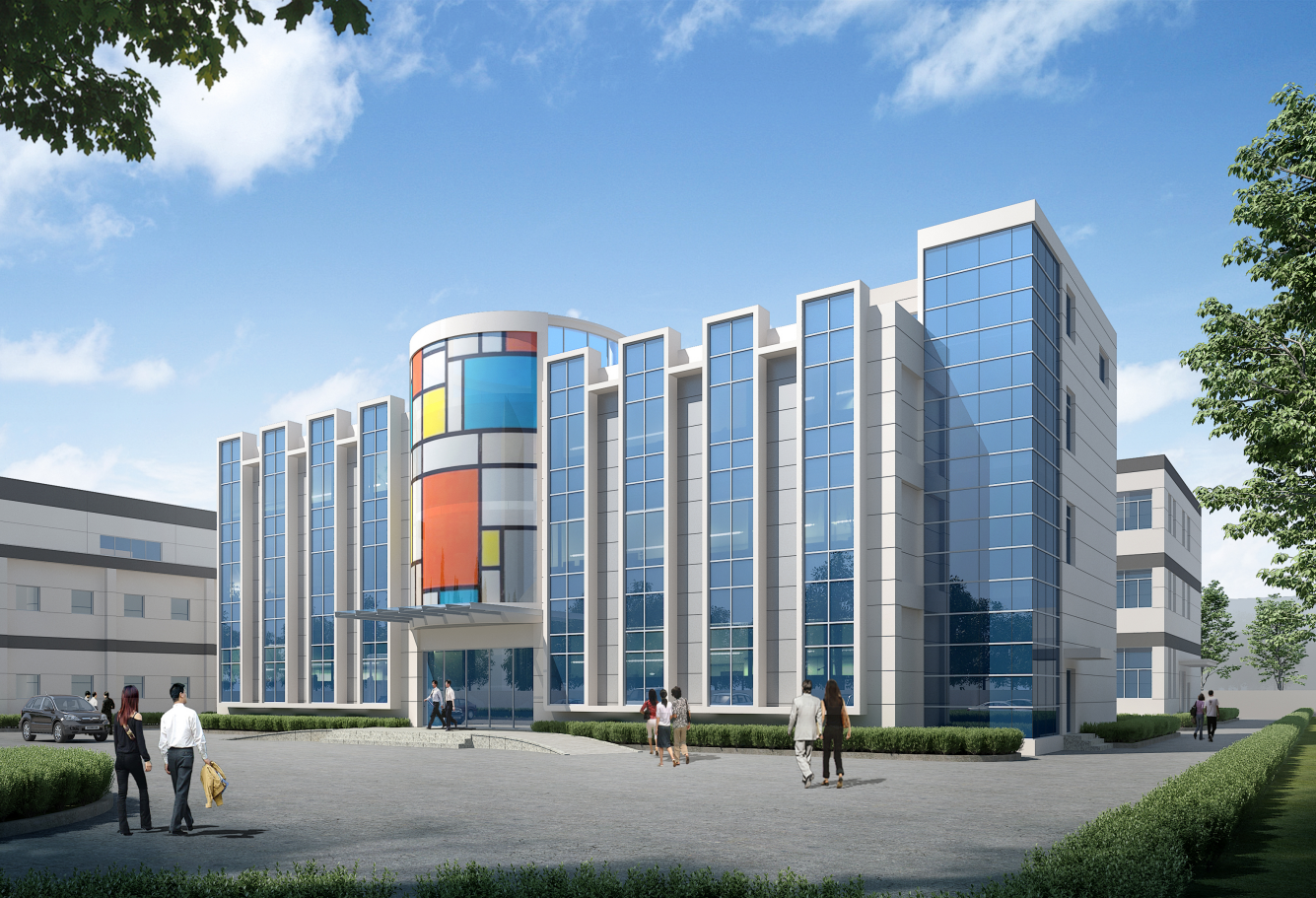
Project: EBU Semiconductor Advanced Packaging Production Line Renovation Project
Location: Baoshan, Shanghai
Duration: 2022–2023
Project Scale: RMB 110.49 million
Delivery Period: 240 days
Scope of Services: MEP systems, specialty gas systems, ultrapure water systems, wastewater, exhaust gas, and waste liquid treatment systems, as well as secondary distribution.
Main Features: The project occupies a total land area of approximately 15,419.5 square meters, with a renovation area of 11,273.6 square meters. It involves the construction of an advanced wafer-level integrated circuit packaging production line with an annual capacity of 720,000 units. The project, with a total investment of RMB 746 million, is funded by Shanghai EBU Semiconductor Co., Ltd. It is located within the Shanghai Robotics Industrial Park, covering 23.01 acres, and includes the establishment of a fan-out wafer-level packaging and testing production line, as well as an advanced silicon photonics wafer-level packaging process experimental platform jointly developed with the Institute of Microelectronics of the Chinese Academy of Sciences.